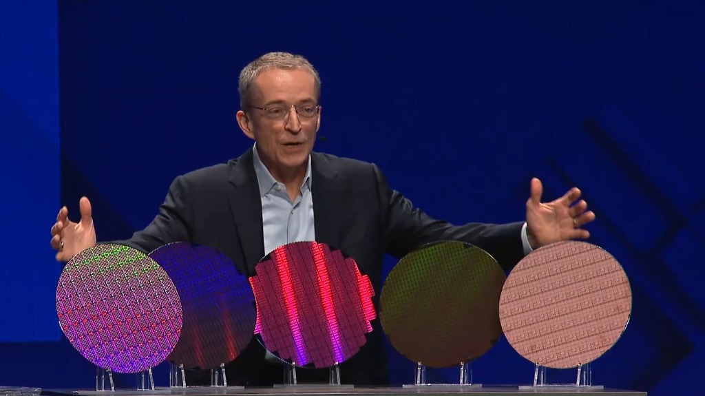
The semiconductor world runs on extremes—precision, cost, and scale that defy imagination. From factories that cost more than aircraft carriers to transistors smaller than viruses, this industry operates at the absolute limits of human engineering. Here are 10 jaw-dropping facts that show just how advanced (and insane) the chip industry really is.
The Semiconductor Industry: Where Extremes Become Reality
The semiconductor industry isn't just another tech sector—it's the most advanced, expensive, and strategically important ecosystem humanity has ever built. Every chip is a masterpiece of physics, precision, and perseverance. These 10 facts reveal the extraordinary scale and complexity of modern chip manufacturing, testing, and validation.
1. The Most Expensive Factories on Earth
The newest TSMC 1.4nm fab in Taichung, Taiwan costs $49 billion USD to build—that's more than three aircraft carriers combined. To put this in perspective, that's enough money to build 130 large hospitals or fund a small country's annual budget.
Why It Matters for Chip Validation
With this level of investment, every chip that comes out of these fabs must be rigorously tested and validated. Hardware testing becomes critical—a single validation error could mean millions in lost revenue. This is why automated chip validation platforms like TestFlow are essential for maximizing yield and catching defects early.
2. More Transistors Than Cells in the Human Body
All fabs combined produce over 2.7 quadrillion transistors every day—far more than the 37 trillion cells in your body. That's 2,700,000,000,000,000 transistors. Every. Single. Day.
The Testing Challenge
Each of these billions of transistors must function perfectly. This creates an unprecedented challenge for semiconductor testing and validation. Modern chips contain billions of transistors that must be validated for functionality, timing, power consumption, and reliability—making automated hardware testing absolutely essential.
3. ASML's EUV Machines: The Most Complex Machines Ever Built
Each High-NA EUV scanner contains 700,000 parts, weighs 180 tonnes, and costs $370 million. There's only one company on Earth that can make them: ASML.
Engineering Marvel: These machines use extreme ultraviolet light with a wavelength of just 13.5 nanometers to pattern features smaller than viruses. The mirrors inside are so smooth that if scaled to the size of Germany, the largest bump would be less than a millimeter high.
4. The Largest Chip Ever Made
The Cerebras Wafer Scale Engine (WSE) packs 4 trillion transistors onto a single wafer-sized chip—the most ever integrated on silicon. This chip is roughly the size of a dinner plate and contains more transistors than 50 NVIDIA H100 GPUs combined.
Validation at Scale
Testing a chip with 4 trillion transistors requires unprecedented validation capabilities. Traditional manual testing methods would take years. This is where AI-powered chip validation becomes essential—automating test generation, execution, and analysis to validate massive chips in reasonable timeframes.
5. Monopolies at the Cutting Edge
The semiconductor industry features unprecedented concentration at the most advanced levels:
- Only one company (ASML) makes EUV lithography machines
- Only one company (TSMC) manufactures over 90% of the world's advanced chips
Strategic Implications: This concentration creates critical dependencies in the global supply chain. Any disruption to ASML or TSMC would impact the entire technology industry, from smartphones to AI servers. This makes reliable chip validation and quality control more important than ever.
6. Transistors Are Incomprehensibly Small
A 2nm transistor is about 12–15nm wide—you could fit 5,000 transistors across the width of a single human hair. To put this in perspective:
Testing at Nanometer Scale
At these scales, quantum effects become significant, and traditional testing assumptions break down. Hardware testing must account for quantum tunneling, thermal variations, and manufacturing tolerances measured in atoms. This requires sophisticated validation methodologies and automated testing platforms.
7. The Water Demand of a Fab
An advanced fab uses up to 5 million gallons of water per day—more than a city of 50,000 people. This water must be ultra-pure, with impurity levels measured in parts per trillion.
Environmental Impact: The semiconductor industry is increasingly focused on water recycling and sustainability. Modern fabs recycle up to 90% of their water, but the sheer volume required highlights the resource intensity of chip manufacturing.
8. Semiconductors Power the Global Economy
Roughly 37% of global GDP depends directly on chips and the systems they enable. From smartphones to data centers, from cars to medical devices, semiconductors are the foundation of the modern economy.
Why Quality Matters
With this level of economic dependence, chip quality and reliability are paramount. A single defective chip in a critical system can have cascading effects. This is why comprehensive hardware testing and chip validation are essential—not just for individual companies, but for the global economy.
9. Approaching the Laws of Physics
A silicon atom is ~0.2 nm wide—meaning we're only about 60 atoms away from the physical limits of transistor scaling. At current 2nm nodes, transistors are already just 75-100 atoms wide.
The End of Moore's Law?
As we approach atomic limits, the industry is shifting to new approaches: 3D stacking, chiplets, new materials (like gallium nitride), and advanced packaging. Each of these innovations brings new validation challenges, requiring more sophisticated hardware testing methodologies and automated chip validation platforms.
10. Cleaner Than Operating Rooms
An advanced fab is 10,000× cleaner than a hospital surgery room—a single dust particle can destroy millions of transistors. Fabs maintain Class 1 cleanrooms, allowing less than 1 particle per cubic foot of air.
Why It Matters: At nanometer scales, even a single dust particle is massive compared to transistor features. Contamination can cause defects that only appear during testing, making rigorous post-silicon validation essential for catching manufacturing issues.
The Testing and Validation Challenge
These extreme facts about the semiconductor industry highlight why hardware testing and chip validation are so critical. When you're working with:
...you can't afford to rely on manual testing methods. The scale, complexity, and economic importance of modern semiconductors demand automated, AI-powered validation platforms that can keep pace with the industry's extremes.
How TestFlow Addresses These Challenges
Scale with Complexity
As chips grow to billions or trillions of transistors, TestFlow's AI-powered test generation scales automatically, creating comprehensive test suites without proportional increases in engineering effort.
Maximize Fab ROI
With fabs costing tens of billions, every chip must meet specifications. TestFlow's automated validation catches defects early, improving yield and maximizing return on massive capital investments.
Handle Nanometer Precision
At 2nm and below, traditional testing assumptions break down. TestFlow's advanced analytics detect subtle issues that manual testing would miss, ensuring quality at atomic scales.
Key Takeaway: Extremes Demand Excellence
The semiconductor industry operates at extremes that most other industries can't even imagine. From the most expensive factories ever built to the smallest functional structures humans have ever created, from monopolistic concentration to global economic dependence—every aspect of this industry pushes the boundaries of what's possible.
These extremes create unprecedented challenges for chip validation and hardware testing. Manual methods simply can't keep up with the scale, complexity, and precision required. The future belongs to automated, AI-powered validation platforms that can match the semiconductor industry's insane standards.
"Every chip is a masterpiece of physics, precision, and perseverance. The semiconductor industry isn't just another tech sector—it's the most advanced ecosystem humanity has ever built."
Want More Semiconductor Insights?
Explore our blog The Semiconductor World for more fascinating deep dives into chip design, manufacturing, testing, and validation. Learn how TestFlow is helping companies navigate the extreme challenges of modern semiconductor development.