System-on-Wafer (SoW) vs. CoWoS: The Packaging Revolution Deciding the AI Race
Everyone argues about 3nm vs 2nm, but the AI race is being decided by packaging. TSMC's move to System-on-Wafer (SoW) promises >40x compute power, but it transforms hardware validation from component testing into a complex system-level challenge.
While the industry fixates on node shrinking—3nm, 2nm, and beyond—the real bottleneck for AI training isn't just transistor density; it's how you connect them. TSMC has thrown down the gauntlet with its System-on-Wafer (SoW) technology, positioning it not just as an upgrade, but as a fundamental architectural shift beyond CoWoS (Chip-on-Wafer-on-Substrate).
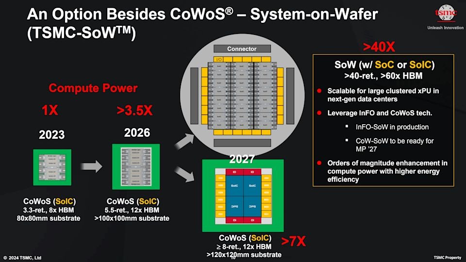
The claims are staggering: >40x compute power and >60x HBM capacity compared to today's baselines. But this shift from "chip + memory" to "manufactured system" introduces profound challenges for hardware validation, packaging verification, and interconnect testing.
From Chip to System: The New Reality
We are moving away from the era where a package was just a protective shell. In the SoW era, the package is the system. Performance is no longer defined solely by the silicon die, but by:
Interconnect Density
The speed and bandwidth of data moving between clustered xPUs.
Memory Proximity
How physically close HBM stacks can sit to the compute cores (SoIC).
Power Delivery
Feeding thousands of amps to a wafer-scale system without voltage droop.
Thermal Limits
Dissipating the heat of an entire server rack concentrated into a single wafer.
The Validation Nightmare (and Opportunity)
With System-on-Wafer, you can't just test individual dies and assume the system works. The complexity of chip testing creates a combinatorial explosion of failure modes.
Packaging Validation
Validating the mechanical stress and electrical integrity of a 12-inch wafer used as a single substrate requires entirely new hardware validation methodologies.
Known Good Die (KGD)
In SoW, one bad chip could potentially ruin the entire wafer-scale system. Pre-bond testing and redundancy logic become mission-critical.
System-Level Test (SLT)
Traditional ATE (Automated Test Equipment) can't handle the power density. We need new system-level testing protocols that mimic real-world AI workloads.
The Roadmap: CoWoS vs. SoW
The Verdict: A Bifurcated Future?
The question isn't whether SoW will replace CoWoS, but rather where the crossover point lies. For most applications, chiplets + CoWoS-style 2.5D packaging will remain the winning architecture due to yield and cost. But for the absolute frontier of AI training—where latency is the enemy—Wafer-Scale systems are becoming inevitable.
As we enter this new era, the "packaging roadmap" is quietly becoming the most important slide in the deck. And for the engineers tasked with validating these behemoths, the job just got a whole lot harder—and a lot more important.
TestFlow 2.0 is live now.Request your access.
Experience the next generation of hardware validation. Run automated test sequences, capture clean data, and accelerate your time-to-market.