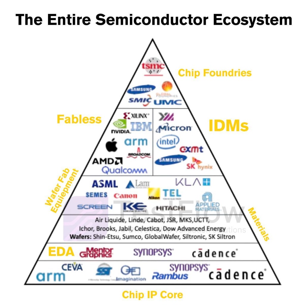
Most people think "chips = TSMC". That’s like saying "movies = Netflix". The semiconductor world is actually a 7-layer stack of deep specialization, where every layer has its own gatekeepers and critical dependencies.
Understanding the semiconductor industry requires looking beyond the finished product. It’s a global relay race where one bottleneck in any layer—design, tools, materials, or validation—can ripple across the entire global economy. Let's break down the 7-layer ecosystem.
1Chip Foundries: The Master Builders
They manufacture chips at insane precision, turning digital designs into physical silicon. These are the most complex factories on earth.
- TSMC (Taiwan)
- Samsung Foundry (Korea)
- SMIC (China)
- GlobalFoundries (USA)
2IDMs (Integrated Device Manufacturers)
Unlike many others, IDMs keep the whole loop—from design to manufacturing—in-house. Companies like Intel, Micron, and SK Hynix are the giants that own their own fabs and design the chips they produce.
3Fabless Chip Designers: The Architects
They design the silicon but hire foundries to build it. They compete on architecture, performance, and software ecosystems.
4Wafer Fab Equipment: The Machine Makers
These companies build the "factories inside the factory". Without ASML's lithography machines or Lam Research's etching tools, the entire industry stops. This is where Moore's Law is actually realized at the physical level.
5Materials + Wafers: The Physical Inputs
Everything starts with ultra-pure silicon wafers and specialty chemicals. Companies like Shin-Etsu, SUMCO, and Linde provide the gases and wafers that form the canvas for chip making.
The Validation Gap
Every layer of this 7-layer stack introduces new points of failure. As we move from EDA tools to Fabless design and eventually to Foundry manufacturing, hardware testing and chip validation are the only things ensuring that what's designed actually works in the real world.
6EDA Software: The Digital Blueprint
Electronic Design Automation (EDA) tools are the software that turn ideas into layouts that foundries can actually fabricate. Synopsys and Cadence dominate this space, providing the logic gates and verification environments for all modern chips.
7Chip IP Cores: The Reusable Logic
Modern chips aren't designed from scratch. Designers license "IP cores" like Arm processor cores or Rambus memory controllers to build their SoC (System on Chip). This layer allows for massive scaling and faster time-to-market.