Intel Installs ASML TWINSCAN EXE:5200B High-NA EUV Machine for 14A Node
Intel Foundry has officially installed ASML’s TWINSCAN EXE:5200B High-NA EUV — the most advanced lithography system ever deployed. This marks a paradigm shift in semiconductor manufacturing and hardware validation strategies for the 14A node.
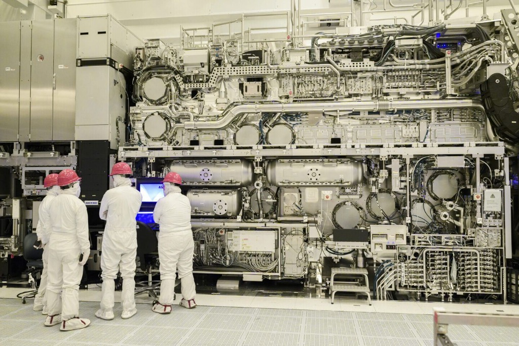
The semiconductor industry has just witnessed a monumental step forward. Intel Foundry has officially installed ASML’s TWINSCAN EXE:5200B High-NA EUV machine, integrating it directly into the manufacturing line for its upcoming 14A node. This isn't just a shiny new tool; it represents the first real industry shift from Low-NA to High-NA EUV, transitioning the technology from an R&D experiment to a critical component of high-volume manufacturing.
For engineers working in hardware validation and chip testing, this development signals a massive simplification in process complexity. By enabling higher resolution patterning, High-NA EUV reduces the need for multi-patterning, potentially decreasing defect rates and streamlining the post-silicon validation process.
Why High-NA EUV Changes Everything
Massive Simplification
One critical layer was reduced from ~40 process steps to fewer than 10. For process validation, this dramatic reduction in steps cuts cycle time and minimizes the opportunities for manufacturing defects to creep in.
Scalable Throughput
The tool already delivers 175 wafers/hour, with Intel targeting 200+ wafers/hour after tuning. Faster throughput means faster wafer sort testing cycles and quicker feedback loops for design teams.
Atomic-Level Precision
Overlay accuracy reaches 0.7 nm — alignment measured at the scale of atoms. This precision is critical for chip verification at advanced nodes, ensuring that hardware design verification matches physical reality.
Stronger Yields, Earlier
Intel reports better yield and performance at this stage of 14A than it had with 18A. Higher initial yields significantly reduce the burden on defect analysis and hardware debugging teams.
Impact on Hardware Testing & Validation
The introduction of High-NA EUV isn't just a manufacturing upgrade; it fundamentally reshapes the hardware validation workflow. With fewer process steps and higher precision, the "noise" creates by manufacturing variations is reduced.
- Reduced Defect Density: Simpler processing implies fewer random defects, allowing chip testing teams to focus on systematic design issues rather than process artifacts.
- Faster Yield Ramps: Improved alignment and reduced complexity accelerate the path to stable yields, shortening the post-silicon validation timeline.
- Tighter Performance Distribution: Atomic precision leads to more consistent transistor performance, simplifying electrical validation and characterization across PVT corners.
Industry Response: Customers Already in the Loop
The shift is already tangible for design teams. The 14A PDK 0.5 is already shipping, and early feedback has been very positive. This enables fabless customers to start their design verification and pre-silicon validation work with confidence in the manufacturing backend.
"This is what progress in semiconductors actually looks like: Fewer steps. Higher yield. Faster cycles. Real physics wins."
High-NA EUV: Production Reality
The installation of the EXE:5200B confirms that High-NA EUV is no longer a distant "next" step—it is officially part of production reality. As the industry pushes towards the 14A node and beyond, the collaboration between advanced lithography and rigorous hardware testing protocols will determine the pace of innovation.
Will High-NA EUV finally reset scaling economics? With the demonstrated simplification of manufacturing steps and early yield wins, it certainly seems poised to raise the bar for what is possible in silicon engineering.
TestFlow 2.0 is live now.Request your access.
Experience the next generation of hardware validation. Run automated test sequences, capture clean data, and accelerate your time-to-market.