Most people think chips are designed. They’re not just designed—they’re manufactured through one of the most complex and unforgiving processes ever built. Turning standard sand into a trillion-transistor processor requires hundreds of precise steps at the atomic level.
The Journey from Sand to Silicon
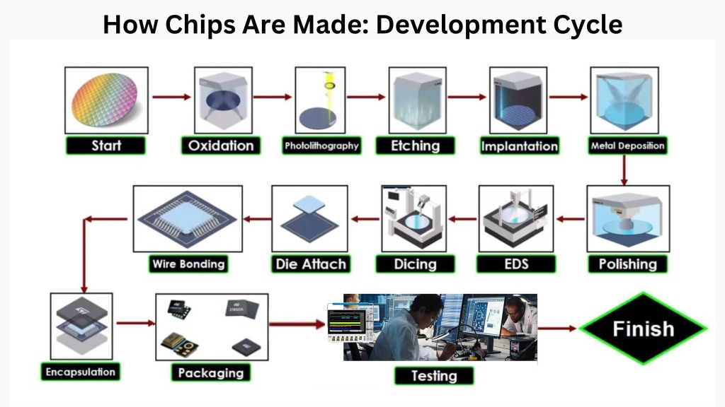
The semiconductor industry doesn't move fast; it moves precisely. Every chip starts with silicon extracted from sand. This raw material undergoes a transformation through a series of stages that challenge the very laws of physics.
1. Wafer Preparation (Oxidation)
The process begins with a pure silicon wafer. A thin oxide layer is grown on the surface to serve as an insulator. This layer is critical for defining the different regions of the chip where electricity will and will not flow.
2. Photolithography
This is where the design comes to life. Using ultra-violet light, engineers "print" extremely small patterns onto the wafer. These patterns define the intricate pathways where billions of transistors will eventually sit. At advanced nodes, this requires EUV (Extreme Ultraviolet) lithography machines that are the most complex machines on earth.
3. Etching & Implantation
After the pattern is printed, unwanted material is etched away with chemical precision. Following this, ions are implanted into the silicon—a process that changes its electrical properties to create the switches we know as transistors. Small variations in this step can destroy the entire wafer's yield.
4. Metallization & Polishing
Transistors are useless unless they are connected. Dozens of metal layers are added, creating a 3D highway of connections for electrons. Between each layer, the wafer is polished perfectly flat so the next layer can be built on top without distortion.
5. Dicing & Packaging
Once the wafer is complete, it is cut (diced) into individual dies. Each functional die is then attached to a substrate, wire-bonded, and encapsulated in a protective package to survive real-world conditions like heat, pressure, and electrical interference.
The Underrated Gate: Testing
And then comes the step many people underestimate: Testing. Every single chip is tested for defects, performance limits, and logical accuracy. At advanced nodes, testing isn't just a final check—it's a massive data-driven operation.
Testing often determines whether a product ships on time or slips by months. It is the bridge between a manufactured hunk of silicon and a functioning product. It starts at the fab with wafer sort testing, continues on automated test equipment in production, and lands in validation labs that increasingly automate the bench with modern LabVIEW alternatives.
Why it causes "Trouble"
- • High-NA EUV complexity requires deeper validation
- • 3D Packaging makes internal nodes harder to reach
- • Yield analysis requires real-time feedback to the fab
The Future of Precision
Semiconductors don't move fast at any one stage—they move precisely through all stages. The complexity of this cycle is why the industry is so capital-intensive. As we move towards sub-2nm nodes, the manufacturing process becomes even more unforgiving, making the role of hardware validation and chip testing exponentially more important.
"Which step in this process do you think causes the most trouble in practice? For most, the answer lies where design meets physical reality—in the validation lab."